NVIDIA
V100S
PCIe
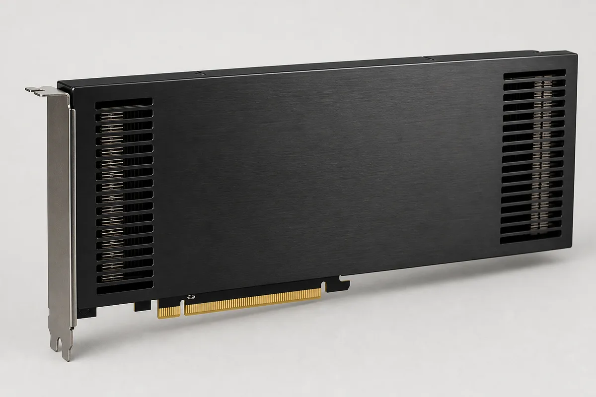
FP32 TFLOPS
16.4 TFLOPS
CUDA Cores
5,120
TDP
250 W
Architecture
Volta
Compute Performance
FP648.2 TFLOPS
FP3216.4 TFLOPS
Architecture
MicroarchitectureVolta
CUDA Cores5120
Tensor Cores640 Tensor Cores
Memory & VRAM
ECC SupportYes
Connectivity & Scaling
InterconnectPCIe
GenerationPCIe Gen3
IB Bandwidth32 GB/s
PCIe InterfaceGen3
Power & Efficiency
TDP250 W
Peak Power250
Thermal LimitsPassive
Physical Design
Form FactorPCIe
FHFLYes
CoolingPassive
Rack DensityMaximum efficiency mode (up to 40% higher compute capacity per rack)
System Compatibility
Required PCIePCIe Gen3
MotherboardPCIe Full Height/Length
Rack Power250 W
Multi-GPU Scalability
Scaling Characteristics
Network BottlenecksPCIe 32 GB/s
Parallelismindependent thread scheduling enables finer-grain synchronization and improves GPU utilization by sharing resources among small jobs
Workload Readiness
Market Authority
Key Strengths
Limitations
Also in the Lineup
Expert Insight
The V100S represents a strategic leap in AI compute. When comparing cloud providers, consider not just the hourly rate, but also the interconnect bandwidth (InfiniBand/NVLink) and regional availability which can significantly impact total cost of ownership for large-scale training.
Glossary Terms
FP32 TFLOPS
VRAM
TDP
Cores
Information updated daily. Cloud pricing subject to vendor availability.